NS 公司的ADC16DV160是双路高速160MSPS模数转换器,采用带数字误差修正的差分流水线架构,片内有取样保持电路,具有极好的动态范围. ADC16DV160具有双数据速率LVDS输出端口,双电源1.8V和3.0V工作,输入范围可在2.4, 2.0, 1.5 和1.0VPP选择,主要用在多载波多标准基站接收器如MC-GSM/EDGE, CDMA2000, UMTS, LTE和WiMAX,,高IF取样接收器,多通路接收器,测试测量设备,通信设备和手提仪表.本文介绍了ADC16DV160主要特性和指标, 功能方框图, 低频输入变压器驱动电路, 高频输入变压器驱动电路和内部基准和去耦电路.
The ADC16DV160 is a monolithic dual channel high performance CMOS analog-to-digital converter capable of converting analog input signals into 16-bit digital words at rates up to 160 Mega Samples Per Second (MSPS). This converter uses a differential, pipelined architecture with digital error correction and an on-chip sample-and-hold circuit to minimize power consumption and external component count while providing excellent dynamic performance. Automatic power-up calibration enables excellent dynamic performance and reduces part-to-part variation, and the ADC16DV160 can be recalibrated at any time through the 3-wire Serial Peripheral Interface (SPI). An integrated low noise and stable voltage reference and differential reference buffer amplifier eases board level design. The on-chip duty cycle stabilizer with low additive jitter allows a wide range of input clock duty cycles without compromising dynamic performance. A unique sample-and-hold stage yields a full-power bandwidth of 1.4 GHz.
The interface between the ADC16DV160 and a receiver block can be easily verified and optimized via fixed pattern generation and output clock position features. The digital data is provided via dual data rate LVDS outputs – making possible the 68-pin, 10 mm x 10 mm LLP package. The ADC16DV160 operates on dual power supplies of +1.8V and +3.0V with a power-down feature to reduce power consumption to very low levels while allowing fast recovery to full operation.
ADC16DV160主要特性:
■ Low power consumption
■ On-chip precision reference and sample-and-hold circuit
■ On-chip automatic calibration during power-up
■ Dual data rate LVDS output port
■ Dual Supplies: 1.8V and 3.0V operation
■ Selectable input range: 2.4, 2.0, 1.5 and 1.0VPP
■ Sampling edge flipping with clock divider by 2 option
■ Integer clock divider by 1 or 2
■ On-chip low jitter duty-cycle stabilizer
■ Power-down and sleep modes
■ Output fixed pattern generation
■ Output clock position adjustment
■ 3-wire SPI
■ Offset binary or 2s complement data format
■ 68-pin LLP package (10x10x0.8, 0.5mm pin-pitch)
ADC16DV160主要指标:
■ Resolution 16 Bits
■ Conversion Rate 160 MSPS
■ SNR
(@FIN = 30 MHz)
(@FIN = 197 MHz)
78.5 dBFS (typ)
76.3 dBFS (typ)
■ SFDR
(@FIN = 30 MHz)
(@FIN = 197 MHz)
95 dBFS (typ)
91.2 dBFS (typ)
■ Full Power Bandwidth 1.4 GHz (typ)
■ Power Consumption
-Core per channel
-LVDS Driver
-Total
591 mW (typ)
118 mW (typ)
1.3W (typ)
■ Operating Temperature Range -40℃~ 85℃
ADC16DV160应用:
■ Multi-carrier, Multi-standard Base Station Receivers
-MC-GSM/EDGE, CDMA2000, UMTS, LTE and WiMAX
■ High IF Sampling Receivers
■ Diversity Channel Receivers
■ Test and Measurement Equipment
■ Communications Instrumentation
■ Portable Instrumentation
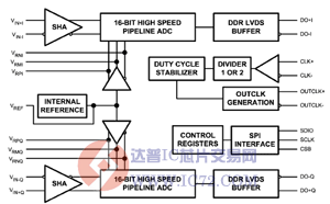
图1.ADC16DV160功能方框图
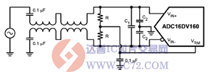
图2.ADC16DV160高频输入变压器驱动电路
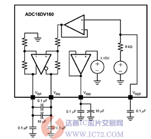
图3.ADC16DV160内部基准和去耦电路图
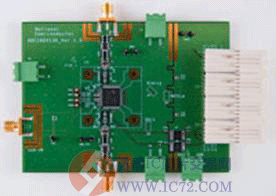
图4.ADC16DV160 评估板外形图