Fairchild 公司的FAN8060是效率高达92%的单片电流模式降压同步稳压器,能从2.5V-5.5V输入电压中提供1A连续电流,输出电压低到1.2V,开关频率1.2MHz,外同步从500kHz到2MHz,占空比100%,可用于PDA,GPS和MP3产品,数码相机,外设端口,DSP核,USB设备,PCMCIA和数据卡等.本文介绍了FAN8060的主要特性,功能方框图以及推荐的应用电路和采用FPF2195 和FAN8060 的GSM/GPRS 调制解调器设计电路.
The FAN8060 is a highly efficient, monolithic, currentmode, step-down synchronous regulator. It can provide 1A continuous current from 2.5V to 5.5V input voltage. The output voltage can be adjusted from 1.2V up to the input voltage with an external voltage divider.
External compensation and soft-start allow for design optimization and flexibility. High-frequency operation allows for all-ceramic solutions and small footprints. In addition, a user-selectable current limit provides protection against output overload and short circuit.
FAN8060 features pulse skipping to achieve higher efficiency during light load operation. 100% duty cycle capability enables power solutions to extend the drop out voltage.
Provision for external synchronization allows users to minimize input capacitors and manage EMI in solutions.
FAN8060 is available in a green, low profile, 10-Lead 3x3mm MLP package.
FAN8060主要特性:
Current Mode Control
Over 96% Efficient
2.5V to 5.5V Input Voltage Range
Output Voltage as Low as 1.2V
1.2MHz Operating Frequency
Less than 1μA Shutdown Current
External Synchronization from 500kHz to 2MHz
100% Duty Cycle
Synchronous Switching FET; no Schottky Diode Required
Stable with Ceramic Capacitors
Light Load Mode with Pulse Skipping
External Compensation
External Soft-Start
Overload / Short-Circuit Protection
Under-Voltage Lockout
Thermal Shutdown
10-Lead 3x3mm Green MLP Package
FAN8060应用:
PDAs
GPS Devices
MP3 Players
Mini PCI
Digital Cameras
Peripheral Ports
DSP Core
USB Devices
PCMCIA
Cable Modem
Data Cards

图1.FAN8060功能方框图
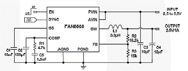
图2.推荐的FAN8060应用电路 (输入5VIN ,输出2.5VO)
Reliable USB Modem Design Using the Combination of an Integrated Load Switch and a Buck Converter
In the portable electronics market, a wireless network allows people to communicate effectively anywhere, at any time, without wires. This is one of the critical factors to consider when designing portable electronics. A wireless modem is a modem that connects to a wireless network instead of a telephone system. Connecting with a wireless modem, attaches directly to a wireless internet services provider.
Global System for Mobile (GSM) and General Packet Radio Service (GPRS) wireless modems, powered by a VBUS line of USB, provide a good method to enable a universal portable device environment. This modem design, however, causes power management issues because the GSM and GPRS transmitters require up to 2A peak current, which exceeds the maximum current capacity of the USB power source. Today, most USB ports are only able to supply up to 1A at 5V. For better reliability, designers must consider several design factors; including input over-current protection (OCP) to avoid overloading the USB power source, a robust step-down converter to make the most of the limited input source, and bulk output capacitors to supply enough power to the pulsed load condition during GSM and GPRS transmission.
The combination of the FPF2195, IntelliMAX load switch, and FAN8060 DC-to-DC converter provides GSM/GPRS modem designers with both input OCP and a maximum output current limit as it satisfies power requirements in a pulsed load. The FPF2195 IntelliMAX is a functional load switch with a 0.15 to 1.5A adjustable current limit and low conductive resistance. The FPF2195 can be mounted on a small PWB (Printed Wiring Board) while maintaining healthy thermal performance. The FAN8060 is a synchronous step-down DC/DC converter operating at 1.2MHz frequency, which allows a low-profile inductor to charge the large output capacitors safely at 95% efficiency.
The FAN8060’s maximum output current protection prevents the shutdown of the hub system during output short conditions.
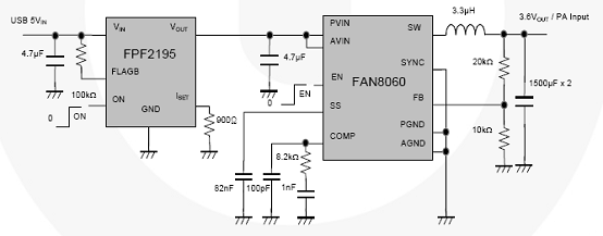
图3.采用FPF2195 和FAN8060 的GSM/GPRS 调制解调器设计电路
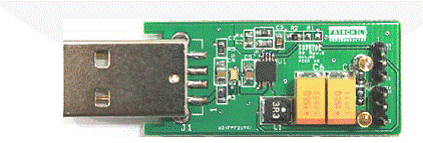
图4.FPF2195和FAN8060 评估板(40mm x 18mm)