ADI公司的ADP1655是非常紧凑的高效双路白光LED闪光驱动器,集成了2MHz同步电感性的升压转换器,I2C兼容的接口和500mA电流源. ADP1655的峰值效率为88%,I2C可编程接口很容易编程定时器,电流和状态位的回读,以便用于工作监视和安全控制. ADP1655可用于照相手机和智能手机,以及数码相机,摄像机和PDA等.本文介绍了ADP1655的主要特性,方框图以及ADP1655评估板系统的主要特性,电路图和材料清单(BOM).
The ADP1655 is a very compact, highly efficient, dual white LED flash driver for high resolution camera phones, which improves picture and video quality in low light environments. The device integrates a 2 MHz synchronous inductive boost convertor, an I2C-compatible interface and a 500 mA current source. The high switching frequency enables the use of a tiny, low profile 2.2 μH power inductor, and the current source permits LED cathode grounding for thermally enhanced, low EMI and compact layouts.
The efficiency is high over the entire battery voltage range to maximize the input power to LED power conversion and minimize battery current draw during flash events. In addition, a Tx-mask input permits the flash LED current to reduce quickly and, therefore, the battery current reduces quickly, during a GSM power amplifier current burst.
The I2C-compatible interface enables the programmability of timers, currents, and status bit readback for operation monitoring and safety control.
The ADP1655 comes in a compact 12-ball 0.5 mm pitch WLCSP package and is specified over the full ?40℃ to +125℃ junction temperature range.
ADP1655主要特性:
Ultracompact solution
Small 2 mm × 1.5 mm 12-ball WLCSP package
Tiny, low profile 2.2 μH power inductor
LED current source for local LED grounding and low EMI
Synchronous 2 MHz PWM boost convertor, no external diode
High efficiency: 88% peak
Reduces high levels of input battery current during flash
Limits battery current drain in torch mode
I2C programmable
Currents up to 400 mA in flash mode for two LEDs
Currents up to 500 mA in flash mode for one LED with 5% accuracy
Currents up to 160 mA in torch mode with 10% accuracy
Peak inductor current limit
Flash timer
Control
I2C-compatible control registers
External STROBE pin
External direct TORCH pin
TX_MASK input to prevent high input battery current levels
Safety
Thermal overload protection Flash timeout Inductor fault detection Output overvoltage Short circuit protection Soft start reduces inrush input current
ADP1655应用:
Camera-enabled cellular phones and smart phones
Digital still cameras, camcorders, and PDAs
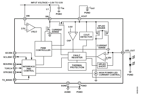
图1.ADP1655方框图
ADP1655评估板系统
The evaluation system is composed of a motherboard and a daughterboard. The motherboard provides the I2C? signals from the computer USB port and generates the I/O voltages and digital high and low signals for the daughterboard. For temperature measurement, the daughterboard can either be plugged directly into the motherboard or connected to the motherboard via the ribbon cable provided with the evaluation kit. The motherboard features a 3.3 V regulator and two adjustable regulators, one for VDDIO and one for ADP1655 supply voltage (VIC). The daughterboard contains numerous jumpers and test points for easy evaluation of the board.
ADP1655评估板主要性:
Input voltage 2.7 V to 5.5 V
Evaluates 1 to 2 LED solutions
Configurable for 2-bit logic or I2C interface
Jumpers for measurement of flash LED current, coil current, and supply current
Evaluation software included
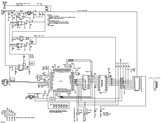
图2.ADP1655评估板电路图(1)
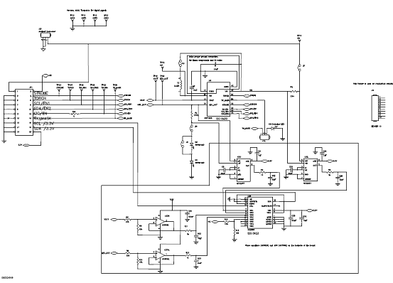
图3.ADP1655评估板电路图(2)