Xilinx公司的Virtex-5 FPGA包括高性能逻辑应用的Virtex-5 LX系列,高性能逻辑和串行连接的Virtex-5 LXT系列,带串行连接的高性能信号处理应用的Virtex-5 SXT系列,有加倍密度的串行连接的高性能系统的Virtex-5 TXT系列和有串行连接的高性能嵌入系统的Virtex-5 FXT系列.而Virtex-5 FXT FPGA ML510开发平台搭配两个整合式PowerPC 440处理器,以及Linux与VxWorks操作系统,能为软件与硬件设计提供弹性与运算容量。ML510内含完备的外围组件、界面、以及软件支持,其中包括支持业界标准Linux与VxWorks操作系统,除两个IBM PowerPC440处理器核心外,机板上的Virtex-5 FX130T组件提供超过13万个逻辑单元、超过10700kb的
block RAM内存、以及运作速度每秒达6.5Gb的RocketIO GTX串行收发器,广泛用在视讯成像、安全通讯以及网路处理等各种嵌入式应用。本文介绍了Virtex-5 FPGA系列的主要特性以及ML510开发平台的主要特性,方框图, 时钟分布图, 嵌入式开发平台方框图和电路图与材料清单(BOM).
The Virtex-5 family provides the newest most powerful features in the FPGA market. Using the second generation ASMBL (Advanced
Silicon Modular Block) column-based architecture, the Virtex-5 family contains five distinct platforms (sub-families), the most choice offered by any FPGA family. Each platform contains a different ratio of features to address the needs of a wide
variety of advanced logic
designs. In addition to the most advanced, high-performance logic fabric, Virtex-5 FPGAs contain many hard-IP system level
blocks, including powerful 36-Kbit
block RAM/FIFOs, second generation 25 x 18 DSP slices, SelectIO
technology with built-in digitallycontrolled impedance, ChipSync source-synchronous interface blocks, system monitor functionality, enhanced clock management tiles with integrated DCM (Digital Clock Managers) and phase-locked-loop (PLL) clock generators, and advanced configuration options.
Additional platform dependant features include power-optimized high-speed serial transceiver blocks for enhanced serial connectivity,
PCI Express compliant integrated Endpoint blocks, tri-mode Ethernet MACs (Media Access Controllers), and high-performance PowerPC 440 microprocessor embedded blocks. These features allow advanced logic designers to build the highest levels of performance and functionality into their FPGA-based systems. Built on a 65-nm state-of-the-art copper process
technology, Virtex-5 FPGAs are a programmable alternative to custom ASIC
technology. Most advanced system
designs require the programmable strength of FPGAs. Virtex-5 FPGAs offer the best solution for addressing the needs of high-performance logic designers, high-performance DSP designers, and high-performance embedded systems designers with unprecedented logic, DSP, hard/soft microprocessor, and connectivity capabilities. The Virtex-5 LXT, SXT, TXT, and FXT platforms include advanced high-speed serial connectivity and link/transaction layer capability.
Virtex-5 FPGA主要特性:
Five platforms LX, LXT, SXT, TXT, and FXT
Virtex-5 LX: High-performance general logic applications
Virtex-5 LXT: High-performance logic with advanced serial connectivity
Virtex-5 SXT: High-performance signal processing applications with advanced serial connectivity
Virtex-5 TXT: High-performance systems with double density advanced serial connectivity
Virtex-5 FXT: High-performance embedded systems with advanced serial connectivity
Cross-platform compatibility
LXT, SXT, and FXT devices are footprint compatible in the same package using adjustable voltage regulators
Most advanced, high-performance, optimal-utilization, FPGA fabric
Real 6-input look-up table (LUT) technology
Dual 5-LUT option
Improved reduced-hop routing
64-bit distributed RAM option
SRL32/Dual SRL16 option
Powerful clock management tile (CMT) clocking
Digital Clock Manager (DCM) blocks for zero delay buffering, frequency synthesis, and clock phase shifting
PLL blocks for input jitter filtering, zero delay buffering, frequency synthesis, and phase-matched clock division
36-Kbit block RAM/FIFOs
True dual-port RAM blocks
Enhanced optional programmable FIFO logic
Programmable
True dual-port widths up to x36
Simple dual-port widths up to x72
Built-in optional error-correction circuitry
Optionally program each block as two independent 18-Kbit blocks
High-performance parallel SelectIO technology
1.2 to 3.3V I/O Operation
Source-synchronous interfacing using ChipSync technology
Digitally-controlled impedance (DCI) active termination
Flexible fine-grained I/O banking
High-speed memory interface support
Advanced DSP48E slices
25 x 18, two’s complement, multiplication
Optional adder, subtracter, and accumulator
Optional pipelining
Optional bitwise logical functionality
Dedicated cascade connections
Flexible configuration options
SPI and Parallel FLASH interface
Multi-bitstream support with dedicated fallback reconfiguration logic
Auto bus width detection capability
System Monitoring capability on all devices
On-chip/Off-chip thermal monitoring
On-chip/Off-chip power supply monitoring
JTAG access to all monitored quantities
Integrated Endpoint blocks for PCI Express Designs
LXT, SXT, TXT, and FXT Platforms
Compliant with the PCI Express Base Specification 1.1
x1, x4, or x8 lane support per block
Works in conjunction with RocketIO transceivers
Tri-mode 10/100/1000 Mb/s Ethernet MACs
LXT, SXT, TXT, and FXT Platforms
RocketIO transceivers can be used as PHY or connect to external PHY using many soft MII (Media Independent Interface) options
RocketIO GTP transceivers 100 Mb/s to 3.75 Gb/s
LXT and SXT Platforms
RocketIO GTX transceivers 150 Mb/s to 6.5 Gb/s
TXT and FXT Platforms
PowerPC 440 Microprocessors
FXT Platform only
RISC architecture
7-stage pipeline
32-Kbyte instruction and data caches included
Optimized processor interface structure (crossbar)
65-nm copper CMOS process technology
1.0V core voltage
High signal-integrity flip-chip packaging available in standard or Pb-free package options
ML510嵌入式开发平台
ML510 Embedded Development Platform
The ML510 series of Embedded Development Platforms offer designers a versatile Virtex-5 FXT platform for rapid prototyping and system verification. In addition to the more than 130,000 logic cells, over 10,700 kb of block RAM, dual IBM PowerPC 440(PPC440) processors, and RocketIO transceivers available in the FPGA, the ML510 provides an onboard Ethernet MAC PHY, DDR2 memory, multiple PCI bus slots, and standard front panel interface ports within an ATX form factor motherboard. An integrated System ACE CompactFlash (CF) controller is deployed to perform board bring-up and to load applications from the CompactFlash card.
The setup and quickstart documentation highlights the functionality of the ML510, using the applications contained on the CompactFlash card. The reference
designs were produced using the
Xilinx Embedded Development Kit (EDK), ISE, and Answer Browser solution records. Tutorials, in coordination with
Xilinx documentation for EDK, ISE, and the Answer Browser, describe how the reference designs and applications were produced. These tutorials can be used to re-create the provided applications and also as a basis for the development of new designs. Xilinx EDK provides for the development of basic board-specific systems, beginning with Base System Builder (BSB), to highly customized systems that leverage the flexibility of Xilinx Platform Studio (XPS) and the EDK intellectual property (IP).
ML510嵌入式开发平台主要特性:
ATX form factor motherboard and ATX-compliant power supply
Dual DDR2 registered DIMMs; each 512 MB density and 72 bits wide
512 MB CompactFlash (CF) card and System ACE CF controller for configuration*
Intel P30 StrataFlash linear flash chip (256 Mb)
Two onboard 10/100/1000 Ethernet PHYs with RJ-45 connectors
PCI Express interface and MIC2592B PCI Express power controller
Two UARTs with RS-232 connectors
DVI graphics interface
LEDs, LCD*, and switches
32/33 PCI subsystem
Two 3.3V slot and two 5V slots
ALi South Bridge SuperIO controller
PS/2 mouse and keyboard connectors
3.5mm headphone and microphone connectors
Two USB peripheral ports
Two serial ATA connectors
Xilinx Personality Module (XPM) interface for access to:
RocketIO GTX transceivers
SPI4.2
GPIO
Power
JTAG and trace debug ports
High-speed I/O through RocketIO GTX transceivers
Encryption battery
Fan controller
Onboard power regulators for all necessary voltages
IIC/SMBus interface*
LTC1694 SMBus accelerator
RTC8566 Real Time Clock (RTC)
64 kb 24LC64 EEPROM
LM87 voltage/temp monitor
Two DDR2 DIMMs with SPD EEPROMs
SPI EEPROM (64 Kb)*
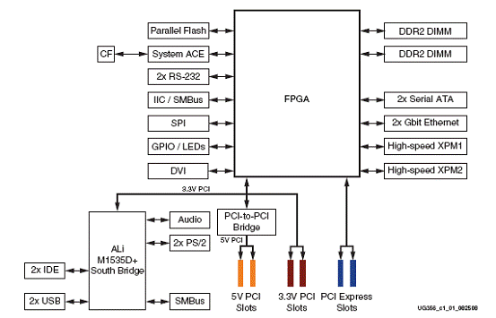
图1.ML510方框图
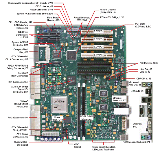
图2.ML510嵌入式开发平台外形图
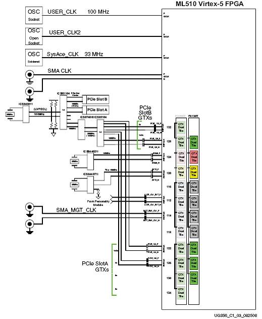
图3.ML510时钟分布图

图4.ML510嵌入式开发平台方框图