ADI 公司的ADP8860是集成了自动光电晶体管控制的可编程背景光LED电荷泵驱动器,能在黑暗和办公室环境光照条件下改变电流强度,从而大大地节省了电源.光强度阈值能通过I2C接口编程,有7路单独和可编程的LED驱动器(6路驱动器电流
30mA,1路驱动器为60mA),可编程最大限流有128等级,待机模式电流小于1uA,主要用于移动显示器背景光和手机键盘背景光,双RGB背景光,LED指示器和小型显示器背景光.本文介绍了ADP8860的主要特性,详细的方框图以及典型应用电路,通用应用电路和带键盘光控制的ADP8860应用电路.
The ADP8860 combines a programmable backlight LED charge pump driver
with automatic phototransistor control. This combi-nation allows for significant
power savings because it changes the current intensity in office and dark ambient light conditions. By performing this
function automatically, it eliminates the need for a processor to monitor the phototransistor.
The light intensity thresholds are fully programmable via the I2C interface. A
second phototransistor input,
with dedicated comparators, improves the ambient light detection levels for various user operating conditions.
The ADP8860 allows as many as six
LEDs to be independently driven up to 30 mA (typical). A seventh LED can be driven to 60 mA (typical). All
LEDs are programmable for minimum/max-imum current and fade in/out times via the I2C interface. These
LEDs can also be combined into groups to reduce the processor instructions during fade in/out.
Driving this entire configuration is a two-capacitor charge pump
with gains of 1×, 1.5×, and 2×. This setup is capable of driving a maximum IOUT of 240 mA from a supply of 2.5 V to 5.5 V. The device includes a variety of safety features including short-circuit, overvoltage, and overtemperature protection. These features allow easy implementation of a safe and robust design. Addi-tionally, input inrush currents are limited via an integrated soft start combined with controlled input-to-output isolation.
The ADP8860 is available in two package types, either a compact 2 mm × 2.4 mm × 0.6 mm WLCSP (wafer level chip scale package) or a small LFCSP (lead frame chip scale package).
ADP8860主要特性:
Charge pump with automatic gain selection of 1×, 1.5×, and 2× for maximum efficiency
Up to two built-in comparator inputs with programmable modes for ambient light sensing
Outdoor, office, and dark modes for maximum backlight
power savings
7 independent and programmable LED drivers
6 drivers capable of 30 mA (typical)
1 driver capable of 60 mA (typical)
Programmable maximum current limit (128 levels)
Standby mode for <1 μA current consumption
16 programmable fade in and fade out times
0.1 sec to 5.5 sec
Choose from linear, square, or cubic rates
Fading override
I2C-compatible interface for all programming
Dedicated reset pin and built-in
power-on reset (POR)
Short-circuit, overvoltage, and overtemperature protection
Internal soft start to limit inrush currents
Input-to-output isolation during faults or shutdown
Operation down to VIN = 2.5 V with undervoltage lockout (UVLO) at VIN = 2.0 V
Small wafer level chip scale package (WLCSP) or lead frame chip scale package (LFCSP)
ADP8860应用:
Mobile display backlighting
Mobile phone keypad backlighting
Dual RGB backlighting
LED indication
General backlighting of small format displays
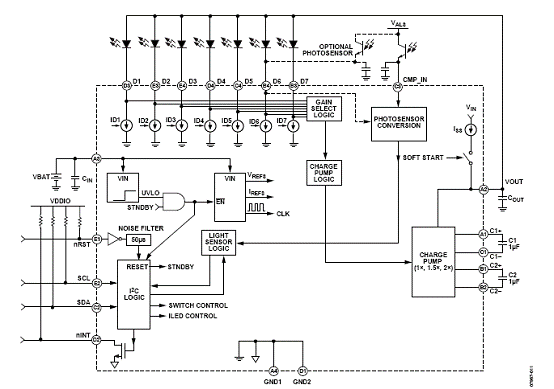
图1.ADP8860详细方框图
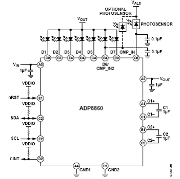
图2.ADP8860典型应用电路

图3.ADP8860通用应用电路
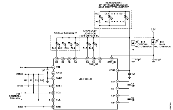
图4.带键盘光控制的ADP8860应用电路