Xilinx 公司的Virtex-5 FPGA是功能强大的FPGA,采用第二代ASMBL列架构,包含有LX, LXT, SXT, TXT和FXT五个平台.每个平台有不同的特性,以满足不同的应用如数据传输和处理,数字视频,嵌入式微处理器,总线接口以及高速设计应用.而ML501评估平台采用 Virtex-5 XC5VLX50-1FFG676 FPGA为主要开发器件.本文介绍了Virtex-5 FPGA 的主要特性以及Virtex-5 FPGA ML501评估平台主要特性和方框图, 电源方框图和评估板详细电路图.
Markets: Industrial, Telecom / Datacom, Medical, Military / Aerospace
Applications: Data Transmission and Manipulation, Digital Video, Embedded Microprocessor, Bus Interface,
High Speed Design
The Virtex-5 family provides the newest most powerful features in the FPGA market. Using the second generation ASMBL (Advanced
Silicon Modular Block) column-based architecture, the Virtex-5 family contains five distinct platforms (sub-families), the most choice offered by any FPGA family. Each platform contains a different ratio of features to address the needs of a wide
variety of advanced logic
designs. In addition to the most advanced, high-performance logic fabric, Virtex-5 FPGAs contain many hard-IP system level blocks, including powerful 36-Kbit block RAM/FIFOs, second generation 25 x 18 DSP slices, SelectIO technology with built-in digitallycontrolled impedance, ChipSync source-synchronous interface blocks, system monitor functionality, enhanced clock management tiles with integrated DCM (Digital Clock Managers) and phase-locked-loop (PLL) clock generators, and advanced configuration options.
Additional platform dependant features include power-optimized high-speed serial transceiver blocks for enhanced serial connectivity, PCI Express compliant integrated Endpoint blocks, tri-mode Ethernet MACs (Media Access Controllers), and high-performance PowerPC 440 microprocessor embedded blocks. These features allow advanced logic designers to build the highest levels of performance and functionality into their FPGA-based systems. Built on a 65-nm state-of-the-art copper process technology, Virtex-5 FPGAs are a programmable alternative to custom ASIC technology. Most advanced system
designs require the programmable strength of FPGAs. Virtex-5 FPGAs offer the best solution for addressing the needs of high-performance logic designers, high-performance DSP designers, and high-performance embedded systems designers with unprecedented logic, DSP, hard/soft microprocessor, and connectivity capabilities. The Virtex-5 LXT, SXT, TXT, and FXT platforms include advanced high-speed serial connectivity and link/transaction layer capability.
Virtex-5 FPGA主要特性:
Summary of Virtex-5 FPGA Features
Five platforms LX, LXT, SXT, TXT, and FXT
Virtex-5 LX:
High-performance general logic applications
Virtex-5 LXT:
High-performance logic with advanced serial connectivity
Virtex-5 SXT: High-performance signal processing applications with advanced serial connectivity
Virtex-5 TXT: High-performance systems with double density advanced serial connectivity
Virtex-5 FXT: High-performance embedded systems with advanced serial connectivity
Cross-platform compatibility
LXT, SXT, and FXT devices are footprint compatible in the same package using adjustable voltage regulators
Most advanced, high-performance, optimal-utilization, FPGA fabric
Real 6-input look-up table (LUT) technology
Dual 5-LUT option
Improved reduced-hop routing
64-bit distributed RAM option
SRL32/Dual SRL16 option
Powerful clock management tile (CMT) clocking
Digital Clock Manager (DCM) blocks for zero delay buffering, frequency synthesis, and clock phase shifting
PLL blocks for input jitter filtering, zero delay buffering, frequency synthesis, and phase-matched clock division
36-Kbit block RAM/FIFOs
True dual-port RAM blocks
Enhanced optional programmable FIFO logic
Programmable
True dual-port widths up to x36
Simple dual-port widths up to x72
Built-in optional error-correction circuitry
Optionally program each block as two independent 18-Kbit blocks
High-performance parallel SelectIO technology
1.2 to 3.3V I/O Operation
Source-synchronous interfacing using ChipSync technology
Digitally-controlled impedance (DCI) active termination
Flexible fine-grained I/O banking
High-speed memory interface support
Advanced DSP48E slices
25 x 18, two’s complement, multiplication
Optional adder, subtracter, and accumulator
Optional pipelining
Optional bitwise logical functionality
Dedicated cascade connections
Flexible configuration options
SPI and Parallel FLASH interface
Multi-bitstream support with dedicated fallback reconfiguration logic
Auto bus width detection capability
System Monitoring capability on all devices
On-chip/Off-chip thermal monitoring
On-chip/Off-chip power supply monitoring
JTAG access to all monitored quantities
Integrated Endpoint blocks for PCI Express Designs
LXT, SXT, TXT, and FXT Platforms
Compliant with the PCI Express Base Specification 1.1
x1, x4, or x8 lane support per block
Works in conjunction with RocketIO™ transceivers
Tri-mode 10/100/1000 Mb/s Ethernet MACs
LXT, SXT, TXT, and FXT Platforms
RocketIO transceivers can be used as PHY or connect to external PHY using many soft MII (Media Independent
Interface) options
RocketIO GTP transceivers 100 Mb/s to 3.75 Gb/s
LXT and SXT Platforms
RocketIO GTX transceivers 150 Mb/s to 6.5 Gb/s
TXT and FXT Platforms
PowerPC 440 Microprocessors
FXT Platform only
RISC architecture
7-stage pipeline
32-Kbyte instruction and data caches included
Optimized processor interface structure (crossbar)
65-nm copper CMOS process technology
1.0V core voltage
High signal-integrity flip-chip packaging available in standard or Pb-free package options
ML501评估平台
The ML501 Evaluation Platform enables designers to investigate and experiment with
features of Virtex-5 LX FPGAs.
ML501 is a feature-rich and low-cost evaluation/development platform which provides easy and practical access to resources available in the on-board Virtex®-5 LX50 FPGA device. Supported by industry standard interfaces and connectors, ML501 is a versatile development platform for multiple applications. The video, audio, and communication ports along with generous memory resources extend the functionality and flexibility of the ML501 beyond a typical FPGA development platform.
Whats Included
ML501 Platform
DVI adapter
CompactFlash Card
Development tools and PC download cable are not included and must be ordered separately
ML501评估平台主要特性:
Key Features
Virtex-5 XC5VLX50-1FFG676 FPGA
64-bit DDR2 small outline DIMM (SODIMM), compatible with EDK supported IP and
software drivers
Programmable system clock generator chip
One differential clock input pair and differential clock output pair with SMA connectors
3.3V clock oscillator socket populated with a 100-MHz oscillator
General purpose DIP switches, LEDs, and pushbuttons
Expansion header with 32 single-ended I/O, 16 LVDS capable differential pairs,
14 spare I/Os shared with buttons and LEDs, power, JTAG chain expansion capability, and IIC bus expansion
Stereo AC97 audio codec with line-in, line-out, 50-mW headphone, microphone-in jacks, and SPDIF digital audio jacks
RS-232 serial port
16-character x 2-line LCD display
One 8-Kb IIC EEPROM
DVI video connector (VGA supported with included adapter)
PS/2 mouse and keyboard connectors
System ACE CompactFlash configuration controller with Type I CompactFlash connector
ZBT synchronous SRAM, 9 Mb on 32-bit data bus with four parity bits
Intel P30 StrataFlash linear flash chips (32 MB)
Serial Peripheral Interface (SPI) Flash (2 MB)
10/100/1000 tri-speed Ethernet PHY transceiver
USB interface chip with host and peripheral ports
Piezo audio transducer
Rechargeable lithium battery to hold FPGA encryption keys
Xilinx XC95144XL CPLD for glue logic
Xilinx XCF32P Platform Flash PROM configuration storage device
JTAG configuration port for use with Parallel Cable III, Parallel Cable IV, or Platform USB download cable
Onboard power supplies for all necessary voltages
Temperature and voltage monitoring chip with fan controller
5V @ 3A AC adapter
Power indicator LED
System monitor
目标应用:
Targeted
ApplicationsMarkets: Industrial, Telecom / Datacom, Medical, Military / Aerospace
Applications: Data Transmission and Manipulation, Digital Video, Embedded Microprocessor, Bus Interface, High Speed Design

图1.Virtex-5 FPGA ML501评估平台方框图

图2.Virtex-5 FPGA ML501评估平台外形图
Detailed Description of Virtex-5 FPGA ML501 Evaluation Platform Components
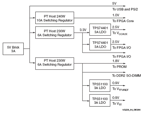
图3.Virtex-5 FPGA ML501评估平台电源方框图
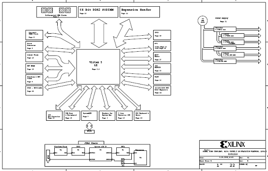
图4.Virtex-5 FPGA ML501评估平台电路图(1)
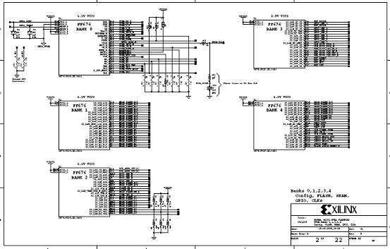
图5.Virtex-5 FPGA ML501评估平台电路图(2)

图6.Virtex-5 FPGA ML501评估平台电路图(3)
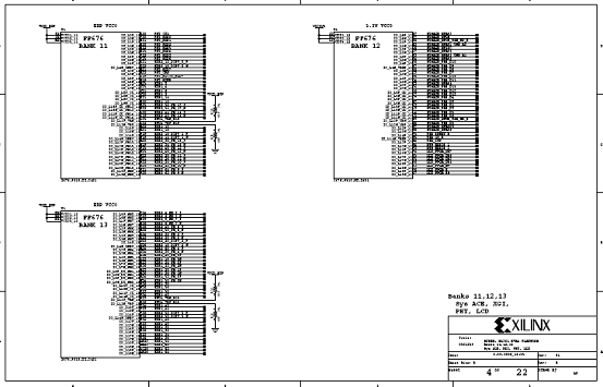
图7.Virtex-5 FPGA ML501评估平台电路图(4)
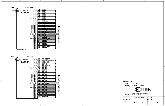
图8.Virtex-5 FPGA ML501评估平台电路图(5)
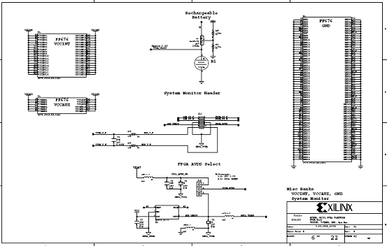
图9.Virtex-5 FPGA ML501评估平台电路图(6)
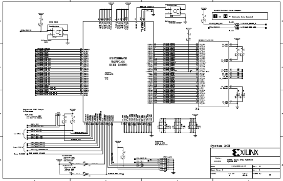
图10.Virtex-5 FPGA ML501评估平台电路图(7)
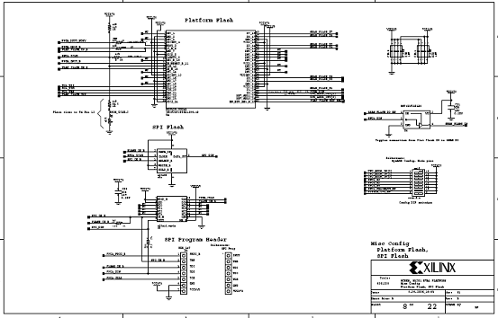
图11.Virtex-5 FPGA ML501评估平台电路图(8)

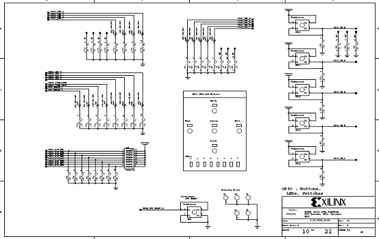
图12.Virtex-5 FPGA ML501评估平台电路图(9)
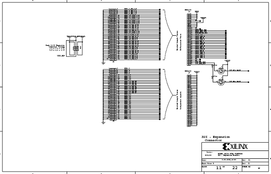
图13.Virtex-5 FPGA ML501评估平台电路图(10)
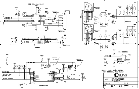
图14.Virtex-5 FPGA ML501评估平台电路图(11)

图15.Virtex-5 FPGA ML501评估平台电路图(12)
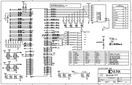
图16.Virtex-5 FPGA ML501评估平台电路图(13)

图17.Virtex-5 FPGA ML501评估平台电路图(14)
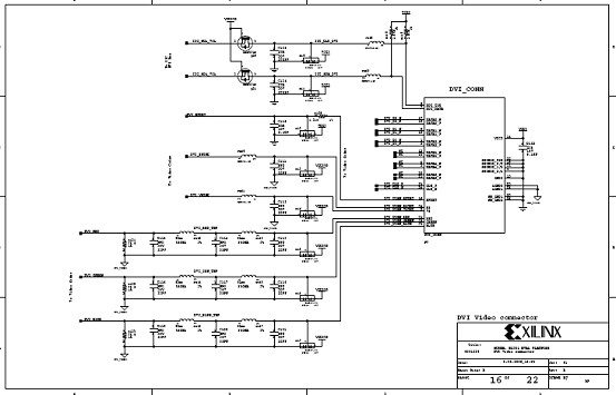
图18.Virtex-5 FPGA ML501评估平台电路图(15)

图19.Virtex-5 FPGA ML501评估平台电路图(16)
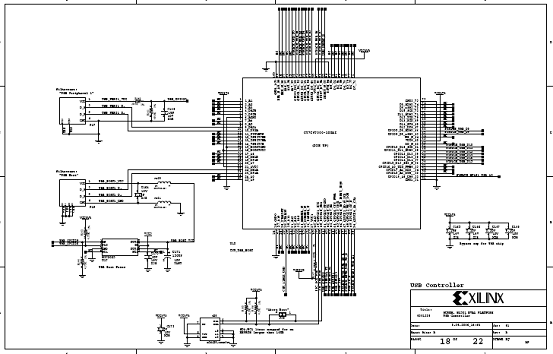
图20.Virtex-5 FPGA ML501评估平台电路图(17)
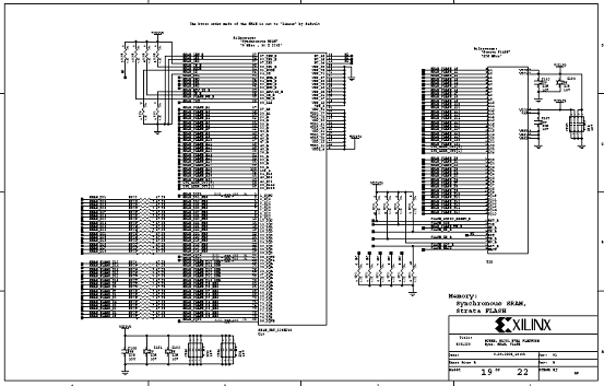
图21.Virtex-5 FPGA ML501评估平台电路图(18)
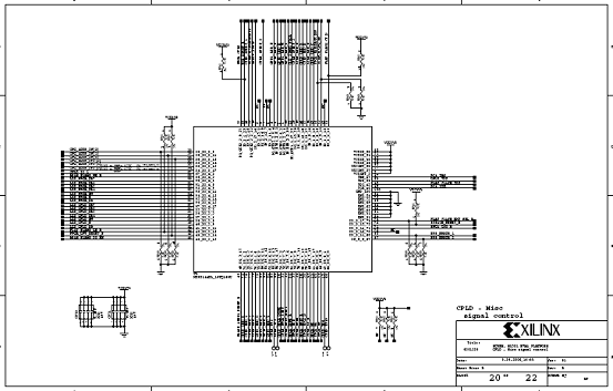
图22.Virtex-5 FPGA ML501评估平台电路图(19)
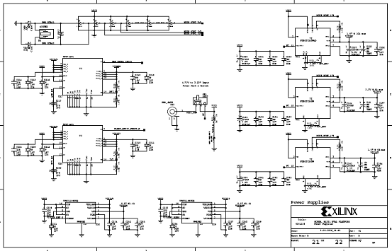
图23.Virtex-5 FPGA ML501评估平台电路图(20)
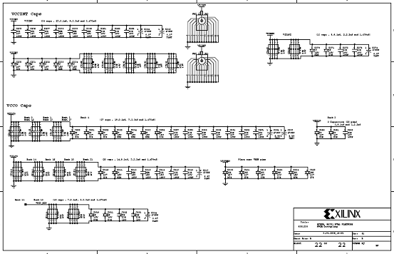
图24.Virtex-5 FPGA ML501评估平台电路图(21)