Linear公司的LTC6416是2GHz低噪音16位ADC缓冲器,有极低的输出噪音和好00MHz以上频率有极好的线性度.差分输入阻抗为12k欧姆,使得可采用1:4和1:8变压器,以增加系统增益.LTC6416的-3dB小信号增益为2GHz,+/-0.1dB带宽为300MHz,输出噪音为1.8nV/√Hz,到300MHz的等效OIP3为40.25dBm,工作电压为2.7V-3.9V,可用在差分ADC驱动器,IF取样接收器,SAW滤波器接口和CCD缓冲器.本文介绍了LTC6416的主要特性,简化方框图,典型应用电路,采用1:4不平衡变压器的差分50欧姆输入阻抗的输入端电路图,采用1:1和4:1不平衡变压器的差分400欧姆负载阻抗的输出端电路图,在140MHz驱动LTC220816位ADC的简化输出端电路图,以及演示板
DC1287A和DC1257B电路图.
LTC64162 GHz Low Noise Differential 16-Bit ADC Buffer.
The LTC 6416 is a differential unity gain buffer designed to drive 16-bit ADCs with extremely low
output noise and excellent linearity beyond 300MHz. Differential input impedance is 12kΩ, allowing 1:4 and 1:8 transformers to be used at the input to achieve additional
system gain.
With no external biasing or gain setting
components and a flow-through pinout, the LTC6416 is very easy to use. It can be DC-coupled and has a common mode
outputoffset of –40mV. If the input signals are AC-coupled, the LTC6416 input pins are internally biased to provide an
output common mode
voltage that is set by the
voltage on the VCM pin.
In addition the LTC6416 has high speed, fast recovery clamping circuitry to limit output signal swing. Both the high and low clamp
voltages are internally biased to allow maximum output swing but are also user programmable via the CLLO and CLHI pins.
Supply current is nominally 42mA and the LTC6416 operates on supply voltages ranging from 2.7V to 3.9V.
The LTC6416 is packaged in a 10-lead 3mm 2mm DFN package. Pinout is optimized for placement directly adjacent to
Linear’s high speed 12-, 14- and 16-bit ADCs.
LTC6416主要特性:
2GHz –3dB Small Signal Bandwidth
300MHz ±0.1dB Bandwidth
1.8nV/√Hz Output Noise
46.25dBm Equivalent OIP3 at 140MHz
40.25dBm Equivalent OIP3 Up to 300MHz
81dBc/–72dBc HD2/HD3 at 140MHz, 2VP-P Out
84.5dBc IM3 at 140MHz, 2VP-P Out Composite
74dBc/–67.5dBc HD2/HD3 at 300MHz, 2VP-P Out
72.5dBc IM3 at 300MHz, 2VP-P Out Composite
Programmable High Speed, Fast Recovery
Output Clamping
DC-Coupled Signal Path
Operates on Single 2.7V to 3.9V Supply
Low Power: 150mW on 3.6V
2mm 3mm 10-Pin DFN Package
LTC6416应用:
Differential ADC Driver
IF Sampling Receivers
Impedance Transformer
SAW Filter Interface
CCD Buffer
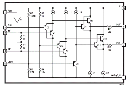
图1.LTC6416简化方框图
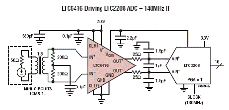
图2.LTC6416典型应用电路
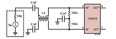
图3.采用1:4不平衡变压器的差分50欧姆输入阻抗的输入端
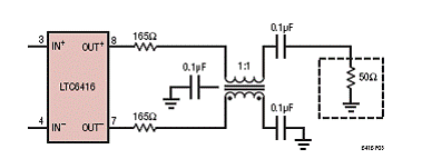
图4.采用1:1不平衡变压器的差分400欧姆负载阻抗的输出端
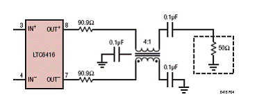
图5.采用4:1不平衡变压器的差分400欧姆负载阻抗的输出端
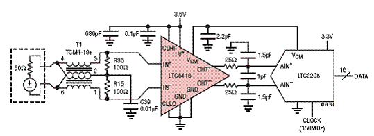
图6.驱动LTC2208 16位ADC(140MHz)的简化输出端电路图
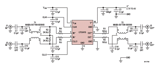
图7.演示板
DC1287A电路图(测试电路A)
图8.演示板DC1257B电路图(测试电路B)