Power one公司的TOPSwitch-HX系列是高性价比的开关电源器件,集成了700V功率MOSFET,高压开关电流源,PWM控制,振荡器,热关断电路,故障保护以及其它控制电路.35W时不需要散热器(P,G和M封装),通用电压输入,在230Vac时可达40W.本文介绍了TOPSwitch-HX的主要特性,几中不同封装产品的方框图以及典型的反激应用框图和35W双输出电源电路图,
150W 19V电源电路图, 20W连续(80W峰值)通用输入电源电路图与65W 19V电源电路图.
TOP252-262 TOPSwitch-HX Family
TOPSwitch-HX cost effectively incorporates a 700 V power MOSFET, high
voltage switched current source, PWM control,
oscillator, thermal shutdown circuit, fault protection and
other control circuitry onto a monolithic device.
TOP252-262器件亮点:
Lower System Cost, Higher
Design Flexibility
Multi-mode operation maximizes efficiency at all loads
New eSIP-7F and eSIP-7C
packagesLow thermal impedance junction-to-case (2 °C per watt)
Low height is ideal for adapters where space is limited
Simple mounting using a
clip to aid low cost manufacturing
Horizontal eSIP-7F package ideal for ultra low height adapter and
monitor applications
Extended package creepage distance from DRAIN pin to adjacent pin and to heat sink
No heatsink required up to 35 W using P, G and M
packages with universal input
voltage and up to 48 W at 230 VAC
Output over
voltage protection (OVP) is user programmable for latching/non-latching shutdown with fast AC reset
Allows both primary and secondary sensing
Line undervoltage (UV) detection prevents turn-off glitches
Line overvoltage (OV) shutdown extends line surge limit
Accurate programmable current limit
Optimized line feed-forward for line ripple rejection
132 kHz frequency (254Y-258Y and all E/L
packages) reduces
transformer and power supply size
Half frequency option for video applications
Frequency jittering reduces EMI fi lter cost
Heatsink is connected to SOURCE for low EMI
Improved auto-restart delivers <3% of maximum power in short circuit and open loop fault conditions
Accurate hysteretic thermal shutdown function automatically recovers without requiring a reset
Fully integrated soft-start for minimum start-up stress
Extended creepage between DRAIN and all
other pins
improves field reliability
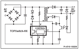
图1.TOPSwitch-HX 典型反激应用框图
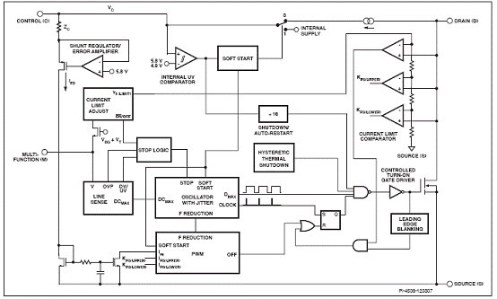
图2.TOPSwitch-HX功能框图(P和 G 封装).
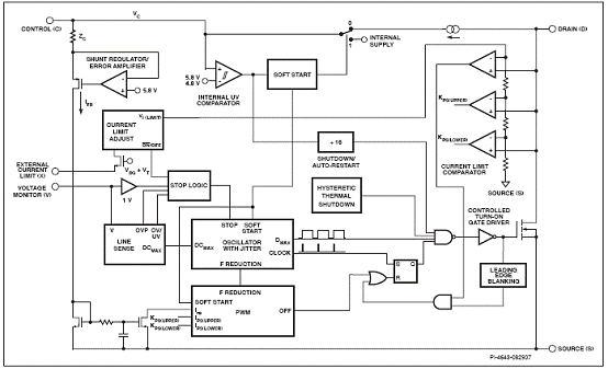
图3.TOPSwitch-HX功能框图(M封装).
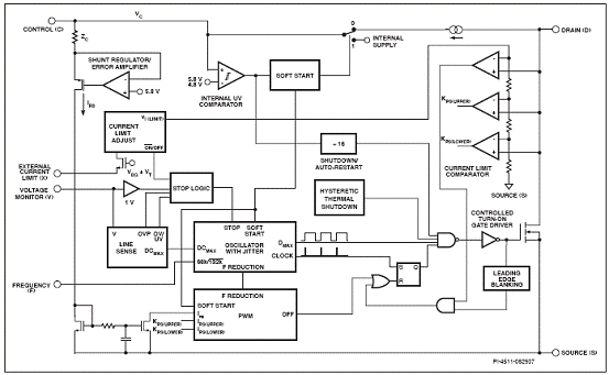
图4.TOPSwitch-HX功能框图(TOP254-258 YN 和所有sSIP封装).
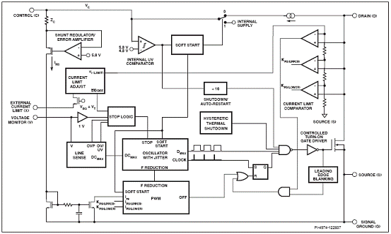
图5.TOPSwitch-HX功能框图(TOP259YN, TOP260YN, TOP261YN)
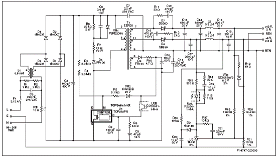
图6.采用TOP258PN的35W双输出电源电路图
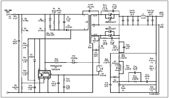
图7.采用TOP258YN的
150W 19V电源电路图
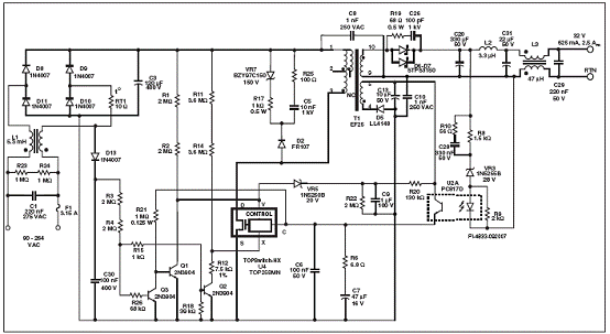
图8.采用TOP258MN的20W连续,80W峰值通用输入电源电路图

图9.采用TOP260EN的65W 19V电源电路图
采用TOP256MN的通用电压输入20W输出反激电源设计
The power supply is a universal input, 20 W output flyback power supply using the TOP256MN device. Typical applications include PC standby power supplies and
other designs needing very low no-load and standby power consumption.
The design is DC input, the rectification/PFC boost stage and EMI filtering provided by the main converter. However the design can be converted to AC input by adding an input inrush thermistor, fuse, bridge rectifier and common mode choke. The efficiency data presented included these components (1 A fuse, 5ohm thermistor, 10 mH common choke and 1 A bridge recifier) to account for any additional losses. The 450 V rating of C1 was selected to provide margin when the supply is fed from a 385 V (nominal) output PFC stage.
Resistors R1 and R2 program the nominal undervoltage (UV) lockout and over-voltage (OV) shutdown limits to 103 VDC and 450 VDC respectively. Resistors R4, R5, and R10 set the current limit over line voltage.
To optimize efficiency under all load conditions U1 operates in one of four modes, from no-load to full load: multi-cycle modulation, fixed frequency PWM (30 kHz), variable frequency PWM and fixed frequency PWM (66 kHz). In all modes the controller maintains a linear relationship between duty cycle and control pin current so that the transition between modes is seamless. For extremely low power levels, U1 operates in the multi-cycle modulation mode (MCM) for excellent low load efficiency and no-load standby
operation
设计亮点:
Very low no-load power consumption <150 mW over entire input voltage range
High efficiency:
>84% efficiency over line and load
Easily meets CEC/ENERGY STAR 2.0
81% and EU CoC 83% average efficiency requirements
77% efficiency at 0.25 A load
Easily meets Energy Star 5.0 2 W input power limit
81% efficiency at 0.60 A load
Easily meets Energy Star 5.0 4 W input power limit
Integrated safety/reliability features:
Accurate, auto-recovering, hysteretic thermal shutdown function maintains safe PCB temperatures under all conditions
Auto-restart protects against output short circuits and open feedback loops
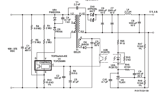
图10. 采用TOP256MN的通用电压输入20W PC待机电源电路图
Universal Input, 20 W Output, PC Standby
Power Supply, Using a TOP256MN Device.
主要设计点:
Clamp capacitor C4 in conjunction with fast diode D5 (FR106,tRR = 500 ns) recycles some of the leakage inductance energy. The observed efficiency gain over a regular Zener clamp is approximately 0.4%. The capacitor also reduces the peak drain voltage by approximately 20 V.
Optocoupler U2 has a high CTR of 300-600%. This reduces the current drawn from the secondary required to move the TOPSwitch-HX into variable frequency, low frequency mode or MCM mode during light load, standby load and no-load conditions.
The transformer T1 is designed such that the design runs in the continuous conduction mode throughout the input voltage operating range. This helps minimizing MOSFET RMS current and thus improves efficiency.
Transformer T1 uses a split two layer primary winding which is wrapped around the bias winding and the secondary winding. This minimizes leakage inductance and primary winding capacitance to improve no-load and standby performance.
To minimize no load consumption, the bias winding turns are selected such that under worst case conditions of load and line the bias voltage is 8 V.
Option:
Using a TLV431 (U3) reduces minimum cathode current for regulation from 400 μA to 55 μA and would remove the need for R15. This would save an additional 10 mW from no-load requirement.