NS公司的SDALTEVK是三速SDI和视频时钟子板卡,专门用于
Altera Cyclone III FPGA的开发套件.SDALTEVK子板卡通过高速子板连接器(HSMC)直接插到Cyclone III开发板, 为广播视频系统设计师提供了完整平台,能块速评估和出设计原型,从而降低产品面市时间.本文介绍了SDALTEVK子板卡的主要特性和优势, SDALTEVK和
Altera Cyclone III主开发板的连接框图以及SDALTEVK子板卡的电路图与材料清单(BOM).
Triple-rate SDI & video clocking daughter
card for
Altera Cyclone III FPGAs National Semiconductor in collaboration
with Altera has developed a triple-rate SDI and video clocking daughter
card for the Altera Cyclone III FPGA development kit (sold separately by Altera). The daughter
card plugs directly into the Cyclone III development board through a High-Speed Mezzanine
Connector (HSMC). The combined solution of the daughter card provides broadcast video system designers a comprehensive platform for rapid evaluation and prototyping of new
designs to reduce time to market.
The SDALTEVK kit consists of:
National Semiconductors HSMC SDI video and clocking daughter card (SDALTEVK)
Comprehensive user manual, schematics, and bill of
materials (BOM)
FPGA IP (not included in box)

图1. SDALTEVK外形图
SDALTEVK Hardware Description
The SDALTEVK daughter card contains:
LMH0344 Triple-rate SDI Adaptive Cable Equalizer
LMH0340 Triple-rate SDI Serializer
with integrated cable driver
LMH0341 Triple-rate SDI deserializer
with reclocked loop through
LMH1981 Multi-Format Video Sync Separator
LMH1982 Multi-Rate Video Clock Generator
DS90CP22 2x2 LVDS Crosspoint Switch
LP3878 Adjustable Low Noise LDO
LM20242 PowerWise Buck Regulator
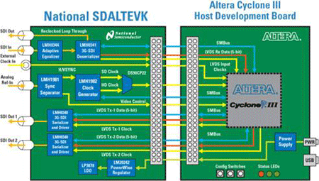
图2.SDALTEVK和Altera Cyclone III主开发板连接框图

图3.SDALTEVK子板卡电路图(1)

图4.SDALTEVK子板卡电路图(2)
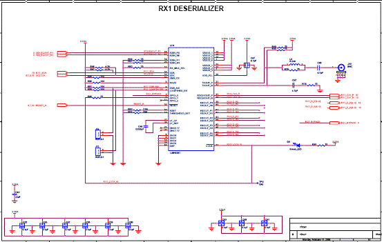
图5.SDALTEVK子板卡电路图(3)
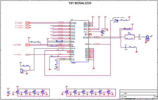
图6.SDALTEVK子板卡电路图(4)
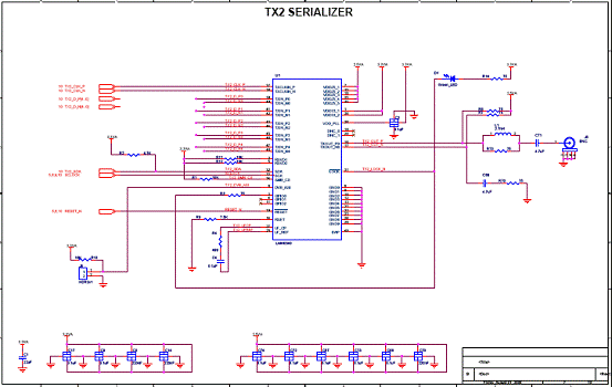
图7.SDALTEVK子板卡电路图(5)

图8.SDALTEVK子板卡电路图(6)
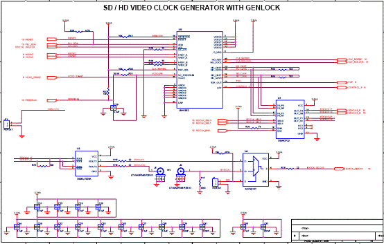
图9.SDALTEVK子板卡电路图(7)

图10.SDALTEVK子板卡电路图(8)
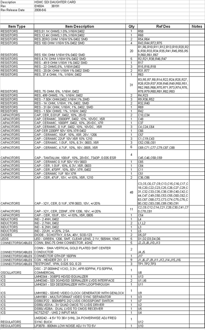
SDALTEVK子板卡材料清单(BOM)见Excel表.