Atmel 公司的AT91SAM9G20是 32位ARM闪存MCU和嵌入MPU,嵌入了以太网MAC,USB设备端口和USB主控制论. AT91SAM9G20采用ARM926EJ-S处理器,并集成了块速ROM和RAM存储器以及大量的外设如USART, SPI, TWI,定时器计数器,同步串行控制器,ADC和多媒体卡接口. AT91SAM9G20的CPU可工作到400MHz,有32KB数据高速缓存和指令高速缓存以及写入缓冲器. AT91SAM9G20具有低功耗和容易使用的特点,广泛应用于系统控制,有线和无线连接,用户接口管理,以及诸如POS终端,安全系统,建筑物自动化,工业控制,医疗和白色家电,PC和手机附件等.本文介绍了AT91SAM9G20的主要特性,方框图以及AT91SAM9G20-EK 评估板详细电路图和材料清单. Atmels AT91SAM 32-bit ARM Flash MCUs and Embedded MPUs are designed for system control, wired & wireless connectivity, user interface management, low power and ease of use. They have received wide acceptance in markets like POS terminals, security, building automation, industrial control, medical, white goods, PC and gaming peripherals, toys and cellular phone accessories. A comprehensive and high-quality eco-system provides access to development tools, Flash programming, software and worldwide technical support. The AT91SAM9G20 is based on the integration of an ARM926EJ-S processor with fast ROM and RAM memories and a wide range of peripherals.The AT91SAM9G20 embeds an Ethernet MAC, one USB Device Port, and a USB Host controller. It also integrates several standard peripherals, such as the USART, SPI, TWI, Timer Counters, Synchronous Serial Controller, ADC and MultiMedia Card Interface. The AT91SAM9G20 is architectured on a 6-layer matrix, allowing a maximum internal bandwidth of six 32-bit buses. It also features an External Bus Interface capable of interfacing with a wide range of memory devices. The AT91SAM9G20 is an enhancement of the AT91SAM9260 with the same peripheral features. It is pin-to-pin compatible with the exception of power supply pins. Speed is increased to reach 400 MHz on the ARM core and 133 MHz on the system bus and EBI. AT91SAM9G20主要特性: Incorporates the ARM926EJ-S ARM Thumb Processor DSP Instruction Extensions, ARM Jazelle Technology for Java Acceleration 32-KByte Data Cache, 32-KByte Instruction Cache, Write Buffer CPU Frequency 400 MHz Memory Management Unit EmbeddedICE, Debug Communication Channel Support Additional Embedded Memories One 64-KByte Internal ROM, Single-cycle Access at Maximum Matrix Speed Two 16-KByte Internal SRAM, Single-cycle Access at Maximum Matrix Speed External Bus Interface (EBI) Supports SDRAM, Static Memory, ECC-enabled NAND Flash and CompactFlash USB 2.0 Full Speed (12 Mbits per second) Device Port On-chip Transceiver, 2,432-byte Configurable Integrated DPRAM USB 2.0 Full Speed (12 Mbits per second) Host and Double Port Single or Dual On-chip Transceivers Integrated FIFOs and Dedicated DMA Channels Ethernet MAC 10/100 Base T Media Independent Interface or Reduced Media Independent Interface 128-byte FIFOs and Dedicated DMA Channels for Receive and Transmit Image Sensor Interface ITU-R BT. 601/656 External Interface, Programmable Frame Capture Rate 12-bit Data Interface for Support of High Sensibility Sensors SAV and EAV Synchronization, Preview Path with Scaler, YCbCr Format Bus Matrix Six 32-bit-layer Matrix Boot Mode Select Option, Remap Command Fully-featured System Controller, including Reset Controller, Shutdown Controller Four 32-bit Battery Backup Registers for a Total of 16 Bytes Clock Generator and Power Management Controller Advanced Interrupt Controller and Debug Unit Periodic Interval Timer, Watchdog Timer and Real-time Timer Reset Controller (RSTC) Based on a Power-on Reset Cell, Reset Source Identification and Reset Output Control Clock Generator (CKGR) Selectable 32,768 Hz Low-power Oscillator or Internal Low Power RC Oscillator on Battery Backup Power Supply, Providing a Permanent Slow Clock 3 to 20 MHz On-chip Oscillator, One up to 800 MHz PLL and One up to 100 MHz PLL Power Management Controller (PMC) Very Slow Clock Operating Mode, Software Programmable Power Optimization Capabilities Two Programmable External Clock Signals Advanced Interrupt Controller (AIC) Individually Maskable, Eight-level Priority, Vectored Interrupt Sources Three External Interrupt Sources and One Fast Interrupt Source, Spurious Interrupt Protected Debug Unit (DBGU) 2-wire UART and Support for Debug Communication Channel, Programmable ICE Access Prevention Mode for General Purpose 2-wire UART Serial Communication Periodic Interval Timer (PIT) 20-bit Interval Timer plus 12-bit Interval Counter Watchdog Timer (WDT) Key-protected, Programmable Only Once, Windowed 16-bit Counter Running at Slow Clock Real-time Timer (RTT) 32-bit Free-running Backup Counter Running at Slow Clock with 16-bit Prescaler One 4-channel 10-bit Analog-to-Digital Converter Three 32-bit Parallel Input/Output Controllers (PIOA, PIOB, PIOC) 96 Programmable I/O Lines Multiplexed with up to Two Peripheral I/Os Input Change Interrupt Capability on Each I/O Line Individually Programmable Open-drain, Pull-up Resistor and Synchronous Output All I/O Lines are Schmitt Trigger Inputs Peripheral DMA Controller Channels (PDC) One Two-slot MultiMedia Card Interface (MCI) SDCard/SDIO and MultiMediaCard Compliant Automatic Protocol Control and Fast Automatic Data Transfers with PDC One Synchronous Serial Controller (SSC) Independent Clock and Frame Sync Signals for Each Receiver and Transmitter I 2 S Analog Interface Support, Time Division Multiplex Support High-speed Continuous Data Stream Capabilities with 32-bit Data Transfer Four Universal Synchronous/Asynchronous Receiver Transmitters (USART) Individual Baud Rate Generator, IrDA Infrared Modulation/Demodulation, Manchester Encoding/Decoding Support for ISO7816 T0/T1 Smart Card, Hardware Handshaking, RS485 Support Full Modem Signal Control on USART0 Two 2-wire UARTs Two Master/Slave Serial Peripheral Interfaces (SPI) 8- to 16-bit Programmable Data Length, Four External Peripheral Chip Selects Synchronous Communications Two Three-channel 16-bit Timer/Counters (TC) Three External Clock Inputs, Two Multi-purpose I/O Pins per Channel Double PWM Generation, Capture/Waveform Mode, Up/Down Capability High-Drive Capability on Outputs TIOA0, TIOA1, TIOA2 One Two-wire Interface (TWI) Compatible with Standard Two-wire Serial Memories One, Two or Three Bytes for Slave Address Sequential Read/Write Operations Master, Multi-master and Slave Mode Operation Bit Rate: Up to 400 Kbits General Call Supported in Slave Mode Connection to Peripheral DMA Controller (PDC) Channel Capabilities Optimizes Data Transfers in Master Mode IEEE 1149.1 JTAG Boundary Scan on All Digital Pins Required Power Supplies 0.9V to 1.1V for VDDBU, VDDCORE, VDDPLL 1.65 to 3.6V for VDDOSC 1.65V to 3.6V for VDDIOP (Peripheral I/Os) 3.0V to 3.6V for VDDUSB 3.0V to 3.6V VDDANA (Analog-to-digital Converter) Programmable 1.65V to 1.95V or 3.0V to 3.6V for VDDIOM (Memory I/Os) Available in a 217-ball LFBGA and 247-ball TFBGA RoHS-compliant Package 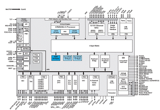 图1.AT91SAM9G20 方框图 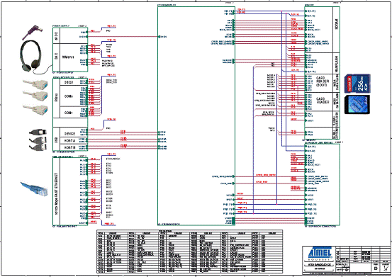 图2.AT91SAM9G20-EK 评估板电路图(1) 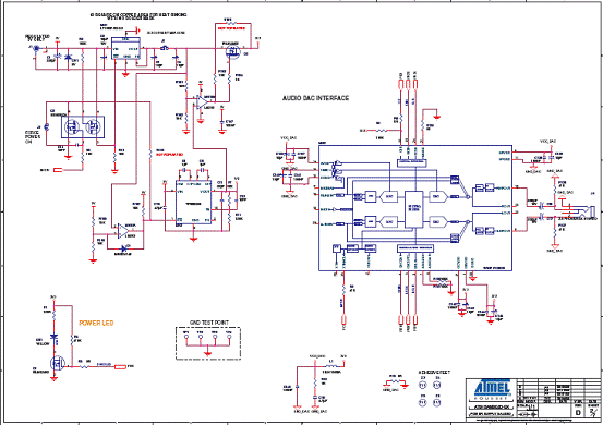 图3.AT91SAM9G20-EK 评估板电路图(2) 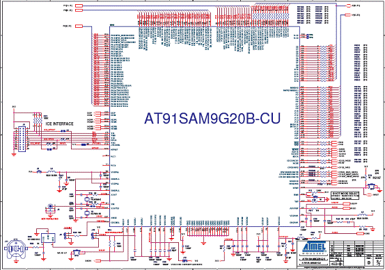 图4.AT91SAM9G20-EK 评估板电路图(3)  图5.AT91SAM9G20-EK 评估板电路图(4) 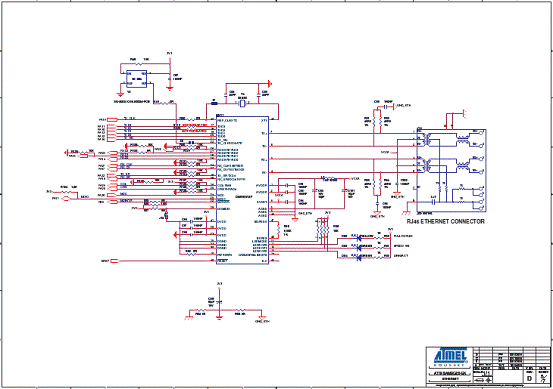 图6.AT91SAM9G20-EK 评估板电路图(5) 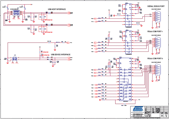 图7.AT91SAM9G20-EK 评估板电路图(6)  图8.AT91SAM9G20-EK 评估板电路图(7) |