TI公司的ADS62Px9/x8系列是双路14位/12位A/D转换器,取样速率高达250
MSPS,具有高动态范围和低功耗特性,在250
MSPS时的功耗为1.25W,串扰为90dB,非常适合用于多载波宽带通信设备.本文介绍了ADS62Px9/x8系列的主要特性,方框图, 模拟输入电路图, 低输入频率, 高输入频率和大于
300MHz的驱动电路图.此外还介绍了ADS62PXX EVM评估板的主要特性,详细电路图和材料清单(BOM).
The ADS62Px9/x8 is a family of dual channel 14-bit and 12-bit A/D converters with sampling rates up to 250
MSPS. It combines high dynamic
performance and low power consumption in a compact 64 QFN package. This makes it well-suited for multi-carrier, wide band-width communications
applications.
The ADS62Px9/x8 has gain options that can be used to improve SFDR
performance at lower full-scale input ranges. It includes a dc offset correction loop that can be used to cancel the ADC offset. Both DDR LVDS (Double Data
Rate) and parallel CMOS digital
output interfaces are available.
It includes internal references while the traditional reference pins and associated decoupling
capacitors have been eliminated. Nevertheless, the device can also be driven with an external reference. The device is specified over the industrial temperature range (-40℃ to 85℃).
ADS62Px9/x8主要特性:
Maximum Sample
Rate: 250 MSPS
14-Bit Resolution - ADS62P49/ADS62P48
12-Bit Resolution - ADS62P29/ADS62P28
Total Power: 1.25 W at 250 MSPS
Double Data
Rate (DDR) LVDS and Parallel CMOS Output Options
Programmable Gain up to 6dB for SNR/SFDR Trade-Off
DC Offset Correction
90dB Cross-Talk
Supports Input Clock Amplitude Down to 400 mVPP Differential
Internal and External Reference Support
64-QFN Package (9 mm × 9 mm)
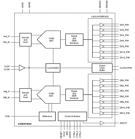
图1.ADS62P49/48 方框图
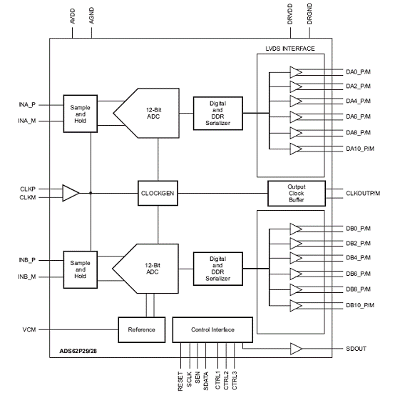
图2.ADS62P29/28 方框图
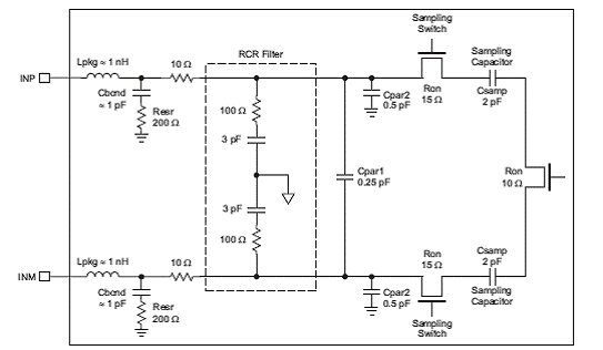
图3.模拟输入电路图
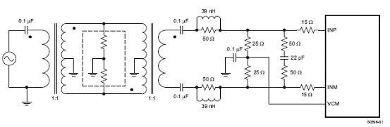
图4.窄带宽驱动电路图 (低输入频率)
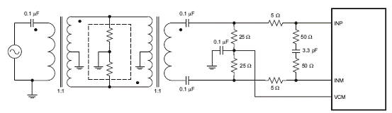
图5.宽带宽驱动电路图(高输入频率)
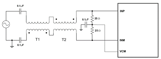
图6.非常高带宽驱动电路(输入频率> 300 MHz)
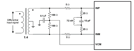
图7.采用1:4 变压器的驱动电路图
ADS62PXX EVM评估板
The ADS62PXX EVM provides a platform for evaluating the analog-to-digital converter (ADC) under various signal, clock, reference and power supply conditions.
The ADS62P49EVM is a circuit board that allows designers to evaluate the
performance of Texas Instruments ADS62P49 device, a dual channel 14-bit 250 MSPS analog to digital converter. The ADC features a user selectable parallel CMOS or DDR LVDS
output. Users can use either the TSW1100 (CMOS mode) or TSW1200EVM (DDR LVDS mode) to capture the data from the converter. The EVM provides a flexible environment to test the ADS62P49 under a variety of clock, input and supply conditions.
The ADS62P49EVM also includes an open socket for Texas Instrument’s new 10 Output Low Jitter Clock Synchronizer and Jitter Cleaner device, the CDCE72010, which can be used to drive the clocking input to the ADS62P49. Open sockets are also provided for an external VCXO and crystal band pass filter allowing for rapid evaluation of a combined high performance ADC and clocking circuit equivalent to a final system level solution. Alternatively an external clock source can be provided to the EVM and either routed through the CDCE72010 or passed directly to the ADS62P49 clock input. By default, the EVM is designed for an external clock source to directly clock the ADS62P49.
The evaluation module also allows designers to use either a transformer coupled input into the ADC or an amplifier input based on the Texas Instruments THS4509. While the ADC EVM comes with the THS4509, users can easily evaluate any of the footprint compatible ADC driving amplifiers such as the THS4508, THS4511 and THS4520.
ADS62PXX EVM评估板主要特性:
USB input for gain settings and other SPI register controls
Transformer coupled analog input path
Transformer coupled clock input path with open socket for CDCE72010 Jitter Cleaner and Clock Synchronizer
Active gain input path based on the THS4509 high speed amplifier
Configurable parallel CMOS or DDR LVDS
output modes
Direct connection to TSW1100 or TSW1200EVM High Speed ADC Evaluation Systems
Separate analog and digital supply connections or single 5V global supply connection
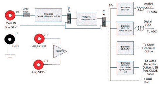
图8. ADS62PXX EVM评估板电源分布图
EVM电路图
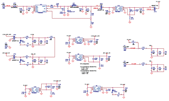
图9. ADS62PXX EVM评估板电路图(1)

图10. ADS62PXX EVM评估板电路图(2)

图11. ADS62PXX EVM评估板电路图(3)
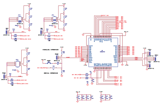
图12. ADS62PXX EVM评估板电路图(4)
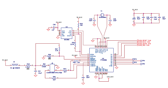
图13. ADS62PXX EVM评估板电路图(5)
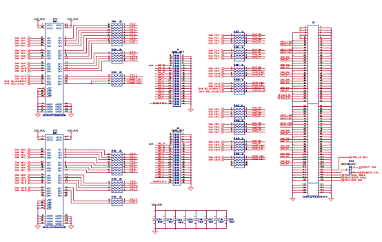
图14. ADS62PXX EVM评估板电路图(6)
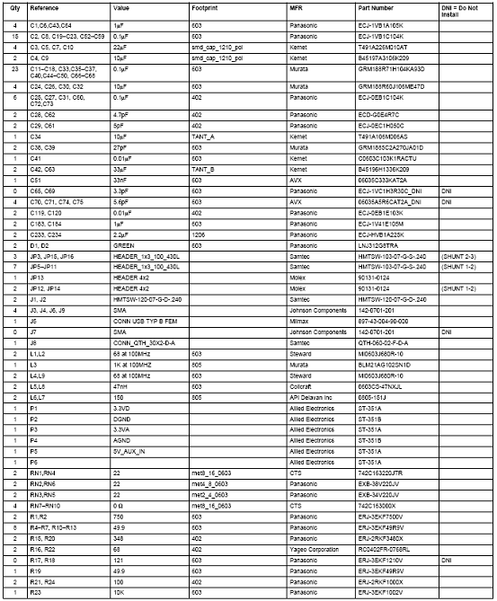
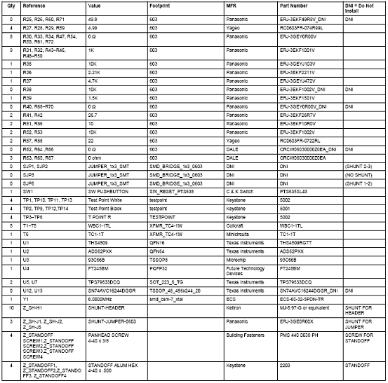
ADS62PXX EVM评估板材料清单(BOM):