NXP 公司的
TDA8025是高性价比的模拟IC卡接口,用于工作在3V,1.8V的异步智能IC卡.
TDA8025集成了电源,保护和控制功能,几乎不需要外接元件,因此有广泛应用如付费电视,电子支付,识别和银行卡阅读器等.本文介绍了
TDA8025的主要特性,方框图以及两种工作电压下的应用方框图.
The TDA8025 is a cost-effective analog interface for asynchronous smart
cards operating at 3 V, 1.8 V or optionally, 1.2 V. Using few external components, the TDA8025 provides
integrated supply, protection and
control functions for a range of applications.
TDA8025主要特性:
Integrated
circuit smart card interface
3 V, 1.8 V or 1.2 V smart card supply
Low power consumption in inactive mode
Three protected, half duplex, bidirectional buffered input/
output lines (C4, C7 and C8)
VCC regulation:
3 V, 1.8 V or optionally 1.2 V at 5 % using one 220 nF and one 470 nF low ESR multilayer ceramic
capacitor.
Current pulse
handling for pulses of 40 nAs at VCC = 3 V, 15 nAs at VCC = 1.8 V or VCC = 1.2 V up to 20 MHz
Thermal and short-
circuit protection for all card contacts
Automatic activation and deactivation sequences triggered by short-
circuit, card take-off, overheating, falling VDD(INTF) and VDD(INTREGD)
Enhanced card-side ElectroStatic Discharge (ESD) protection of > 6 kV
Clock signal using the internal oscillator or an external crystal (26 MHz) connected to pin XTAL1
Card
clock generation up to 20 MHz with synchronous frequency changes of fxtal,12 fxtal, 14 fxtal or 18 fxtal using pins CLKDIV1 and CLKDIV2
Non-inverted
control of pin RST using pin RSTIN
NDS certified
Supply supervisors during power on and off:
VDD(INTREGD) using a fixed threshold
VDD(INTF) using resistor bridge threshold adjustment
Built-in debouncing on card presence contacts (typically 4.5 ms)
Multiplexed status signal using pin OFFN
TDA8025应用:
Pay TV
Electronic payment
Identification
Bank card readers

图1.TDA8025方框图
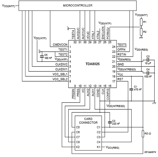
图2.TDA8025应用框图(3 V < VDDI(REG) < 3.6 V)

图3.TDA8025应用框图(3.6 V < VDDI(REG) < 5.5 V)